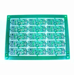
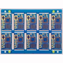
Printed Circuit Board popularly known as PCB is a board which is made up of a very thin flat metal or hard plastic type board and upon which so many electronic components are mounted. The basic function of it is to provide continuous mechanical support to the machine.
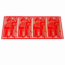
It is now used in all sorts of mechanical and electronic products such as automobiles, cellular telephones, personal computers etc. This is the reason why PCB manufacturing companies are widely spread now a day.
The technology of PCB Fabrication has become more advanced in the present context. It consists of following steps:
1 Initially PCBs are fabricated with two Softwares CAD and CAM to produce the PCB prototype.
2. Then the material of the PCB is selected.
3. Then a coating of copper is applied to the entire board.
4. In the next step, the circuit layout is printed on the board by a photosensitive process which results are the traces or tracks of the PCB circuit.
5. To connect the circuit traces, two processes are used. One is mechanical milling process and the other is an etch-resistant, silkscreen, printing process.
6. Then to mount the components, holes must be drilled at the points where the electrical and electronics parts are placed on the board.
7. Once the holes are drilled, hollow rivets are inserted into them or they are coated by an electroplating process, which creates the electrical connection between the layers of the board. A masking material is then applied to coat the entire PCB with the exception of the pads and the holes.
8. The final step is to screen print the board so labels and the legend appear at their proper locations.
Ace Electech Ltd. is an advanced quick turn PCB manufacturer which have years of expertise in manufacturing and supplying of quality PCBs. So visit our website and place your purchase order. You will get your desired PCB with specification at a cheaper price.
 RSS Feed
