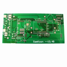
Use of PCB in the technological world is at very high. The basic function of it is to provide continuous mechanical support to the machine. It is now used in all sorts of mechanical and electronic products such as automobiles, cellular telephones, personal computers etc. In PCB manufacturing various raw materials are being used but copper is considered as the basic material.
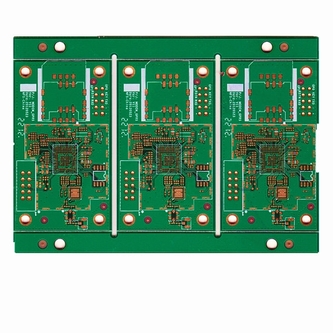
Generally copper is always coated using a tin-lead combination to protect it from oxidation. PCBs can be single layered, double layered or multi layered using the techniques such as PCB milling, copper etching, screen printing etc basing on the requirement of the customers.
PCB fabrication is a key process in the manufacturing of PCBs. But before that PCB prototype remains made ready. The step by step of PCB fabrication is as described below.
1. Initially PCBs are fabricated with two softwares CAD and CAM to produce the PCB prototype.
2. Then the material of the PCB is selected and coated with copper.
3. In the next step, the circuit layout is printed on the board by a photosensitive process.
4. Then the circuit traces are connected.
5. Then to mount the components, holes must be drilled at the points where the electrical and electronics parts are placed on the board.
6. Once the holes are drilled, hollow rivets are inserted into them or they are coated by an electroplating process. A masking material is then applied to coat the entire PCB with the exception of the pads and the holes.
7. The final step is to screen print the board so labels and the legend appear at their proper locations.
ACE ELECTECH LTD is a professional quickturn PCB manufacture It has created a successful track record by its competent product and service delivery. So contact us in our website and place your purchase order online to get the error free PCBs.
 RSS Feed
